Atomically Precise Graphene Nanoribbon Devices
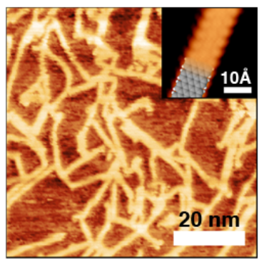
Figure 1. STM of synthesized GNRs
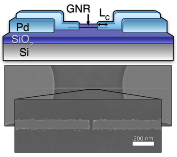
Figure 2. Fabricated GNRFET
Chemically synthesized graphene nanoribbons (GNRs) present an attractive alternative to carbon nanotubes as high performance semiconducting channel material. Because of their deterministic growth process, these GNRs possess identical electronic properties en masse and, unlike other GNRs, lack rough edges that potentially reduce mobility and transport.
Our group develops the techniques required to integrate these GNRs into electronic devices, enabling us to measure and characterize their electronic response directly through transport and optical spectroscopy. Working directly with chemists and physicists, we are developing new synthesis methods and precursors that improve device performance and yield, while also developing fabrication techniques that enable electrical probing of molecular heterojunctions at the nanometer scale.